| CPC H01L 25/0655 (2013.01) [H01L 24/06 (2013.01); H01L 24/08 (2013.01); H01L 24/09 (2013.01); H01L 24/17 (2013.01); H01L 24/29 (2013.01); H01L 24/30 (2013.01); H01L 25/0652 (2013.01); H01L 2224/08225 (2013.01); H01L 2224/09177 (2013.01); H01L 2224/81 (2013.01)] | 18 Claims |
|
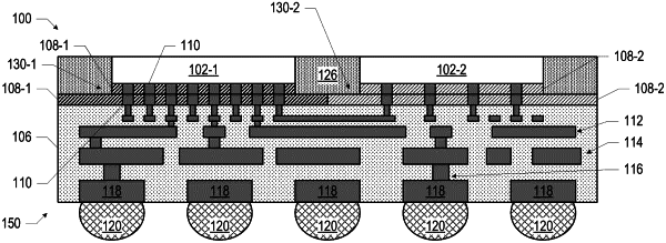
1. A microelectronic assembly, comprising:
a first microelectronic component; and
a second microelectronic component coupled to the first microelectronic component by a direct bonding region, wherein the direct bonding region includes a first subregion and a second subregion, and the first subregion has a greater metal density than the second subregion, wherein the first subregion includes a first dielectric material, the second subregion includes a second dielectric material, and a material composition of the first dielectric material is different from a material composition of the second dielectric material.
|