| CPC H01L 24/83 (2013.01) [H01L 24/32 (2013.01); H01L 2224/32225 (2013.01); H01L 2224/83051 (2013.01); H01L 2224/83141 (2013.01); H01L 2224/83191 (2013.01); H01L 2224/83192 (2013.01)] | 2 Claims |
|
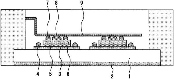
1. A semiconductor device comprising:
an insulating substrate including an electrode;
an alignment resin provided in an annular shape on the electrode;
solder having a thickness thinner than that of the alignment resin and arranged on the electrode on an inner side of the annular shape of the alignment resin; and
a semiconductor chip bonded to the electrode using the solder,
wherein the alignment resin is arranged as a plurality of dots around a periphery of the chip to form the annular shape.
|