| CPC H01L 24/82 (2013.01) [H01L 24/20 (2013.01); H01L 24/29 (2013.01); H01L 24/45 (2013.01); H01L 24/83 (2013.01); H01L 24/85 (2013.01); H01L 2224/82203 (2013.01); H01L 2924/1431 (2013.01); H01L 2924/1434 (2013.01)] | 20 Claims |
|
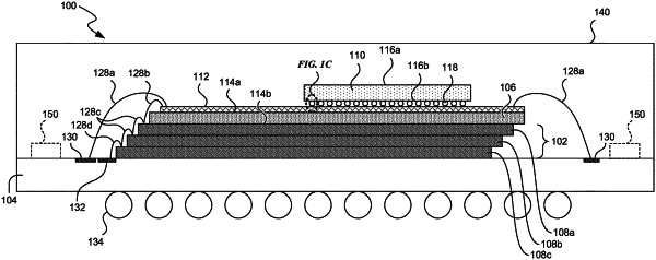
1. A semiconductor assembly, comprising:
a die stack including a plurality of semiconductor dies;
a routing substrate mounted on the die stack, the routing substrate including an upper surface facing away from the die stack;
a redistribution structure formed above the upper surface of the routing substrate;
a plurality of electrical connectors coupling the redistribution structure to at least some of the plurality of semiconductor dies of the die stack; and
a controller die mounted on the routing substrate electrically coupled to the redistribution structure, wherein the plurality of semiconductor dies are electrically coupled to the controller die via the redistribution structure.
|