| CPC H01L 24/75 (2013.01) [H01L 24/83 (2013.01); H01L 2224/7565 (2013.01); H01L 2224/75753 (2013.01)] | 12 Claims |
|
1. An apparatus for semiconductor device bonding, the apparatus comprising:
(a) a gantry assembly comprising a gantry actuation mechanism;
(b) a base assembly for supporting at least one substrate;
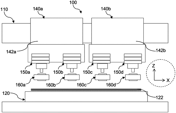
(c) at least one bonding assembly attached to the gantry assembly and positioned above the base assembly, the at least one bonding assembly comprising two or more bonding heads and a bonding assembly actuator, wherein the gantry actuation mechanism moves and positions the two or more bonding heads horizontally planarly and the bonding assembly actuator moves and positions the two or more bonding heads vertically, the two or more bonding heads configured for concurrently picking up and moving a plurality of semiconductor devices both horizontally planarly along an X-axis and a Y-axis and vertically, and concurrently bonding the plurality of semiconductor devices at respective bonding locations on the at least one substrate; and
(d) at least one vision assembly attached to the gantry assembly and moved by the gantry actuation mechanism concurrently with the two or more bonding heads, the at least one vision assembly comprising a plurality of pairs of alignment cameras, each pair of alignment cameras comprising an uplook camera configured to look vertically upward to target sight and capture an upward reference view of a corresponding one of the plurality of semiconductor devices picked up by the corresponding one of the two or more bonding heads, and a downlook camera axially aligned to the uplook camera to look vertically downward to target sight and capture a downward reference view of a corresponding bonding location on the at least one substrate, wherein the plurality of semiconductor devices are aligned by micro movements of a portion of the two or more bonding heads relative to the respective bonding locations, based on the upward and downward reference views captured by the respective pairs of alignment cameras thereby concurrently aligning the plurality of semiconductor devices to correct for an alignment offset with the corresponding bonding locations on the at least one substrate.
|