| CPC H01L 24/17 (2013.01) [H01L 21/4853 (2013.01); H01L 21/486 (2013.01); H01L 21/563 (2013.01); H01L 21/565 (2013.01); H01L 21/6835 (2013.01); H01L 23/3128 (2013.01); H01L 23/3135 (2013.01); H01L 23/49827 (2013.01); H01L 23/49838 (2013.01); H01L 23/562 (2013.01); H01L 24/08 (2013.01); H01L 24/16 (2013.01); H01L 24/80 (2013.01); H01L 25/0655 (2013.01); H01L 25/50 (2013.01); H01L 2221/68331 (2013.01); H01L 2224/08225 (2013.01); H01L 2224/16227 (2013.01); H01L 2224/17517 (2013.01); H01L 2224/80895 (2013.01); H01L 2224/80896 (2013.01); H01L 2924/3511 (2013.01)] | 20 Claims |
|
1. A method comprising:
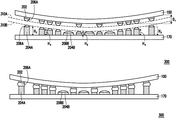
forming a first redistribution structure on a first side of an interposer, the first redistribution structure comprising metal lines and vias in dielectric layers, the first redistribution structure comprising active pads and dummy pads on a first surface of the first redistribution structure, the active pads being electrically coupled to the metal lines and vias, the dummy pads being electrically isolated from the metal lines and vias;
forming active connectors on the active pads;
forming dummy connectors on the dummy pads;
attaching a first integrated circuit device to a first subset of the active connectors;
attaching a second integrated circuit device to a second subset of the active connectors, the dummy connectors being between the interposer and the second integrated circuit device;
forming an underfill on the first side of the interposer, the underfill having a first portion beneath the first integrated circuit device and a second portion beneath the second integrated circuit device; and
encapsulating the first integrated circuit device and the second integrated circuit device with an encapsulant.
|