| CPC H01L 24/16 (2013.01) [H01L 23/49838 (2013.01); H01L 24/17 (2013.01); H01L 2224/16225 (2013.01); H01L 2224/1713 (2013.01); H01L 2924/30101 (2013.01)] | 21 Claims |
|
1. A semiconductor device, comprising:
a semiconductor die mounted at a die area of a package with an array of electrically-conductive balls providing electrical contact for the semiconductor die; and
a power channel to convey a power supply current to the semiconductor die;
wherein the power channel comprises:
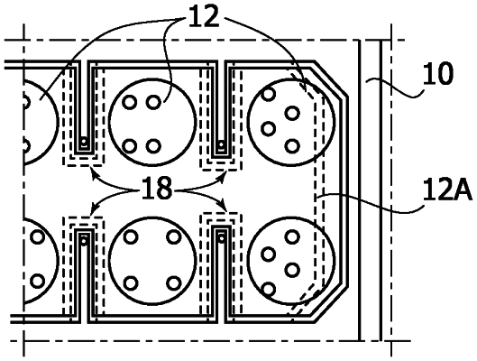
at least one electrically-conductive connection plane layer extending in a longitudinal direction of the electrically-conductive connection plane layer between a distal end at the periphery of the package and a proximal end at the die area of the package; and
wherein said array of electrically-conductive balls includes a distribution of electrically-conductive balls distributed along the longitudinal direction of the electrically conductive connection plane layer;
said electrically-conductive connection plane layer comprising subsequent portions in said longitudinal direction between adjacent electrically-conductive balls in said distribution;
wherein said subsequent portions have respective electrical resistance values, wherein said respective electrical resistance values decrease from said distal end to said proximal end of the electrically-conductive connection plane layer;
wherein the electrically-conductive connection plane layer comprises voids formed therein between adjacent electrically-conductive balls in said distribution, wherein said voids define therebetween said subsequent portions of the electrically-conductive connection plane layer having respective electrical resistance values; and
wherein said voids filled with ground material.
|