| CPC H01L 24/16 (2013.01) [H01L 23/481 (2013.01); H01L 24/04 (2013.01); H01L 24/17 (2013.01); H01L 24/32 (2013.01); H01L 24/33 (2013.01); H01L 24/73 (2013.01); H01L 25/0652 (2013.01); H01L 25/0657 (2013.01); H01L 2224/02372 (2013.01); H01L 2224/0401 (2013.01); H01L 2224/16146 (2013.01); H01L 2224/16227 (2013.01); H01L 2224/1703 (2013.01); H01L 2224/17132 (2013.01); H01L 2224/17181 (2013.01); H01L 2224/17183 (2013.01); H01L 2224/32225 (2013.01); H01L 2224/33181 (2013.01); H01L 2224/33183 (2013.01); H01L 2224/73204 (2013.01); H01L 2225/06513 (2013.01); H01L 2225/06517 (2013.01)] | 18 Claims |
|
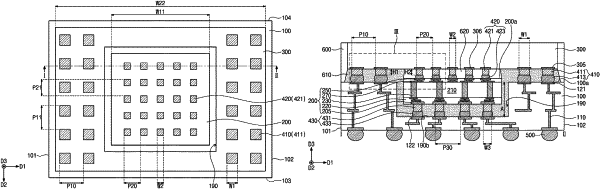
1. A semiconductor package, comprising:
a package substrate that extends in a first direction and a second direction perpendicular to the first direction and that includes a recessed portion on a top surface of the package substrate;
a lower semiconductor chip in the recessed portion of the package substrate;
an upper semiconductor chip on the lower semiconductor chip and the package substrate, the upper semiconductor chip having a width greater than a width of the lower semiconductor chip, in the first direction;
a plurality of first bumps directly between the package substrate and the upper semiconductor chip; and
a plurality of second bumps directly between the lower semiconductor chip and the upper semiconductor chip,
wherein a pitch of the second bumps is less than a pitch of the first bumps, in the first direction,
wherein each of the first bumps includes:
first solder part on the package substrate; and
a first pillar pattern between the first solder part and the upper semiconductor chip,
wherein each of the second bumps includes:
a second solder part on the lower semiconductor chip; and
a second pillar pattern between the second solder part and the upper semiconductor chip, and
wherein, in a third direction perpendicular to the first direction and the second direction, a height of the second solder part is less than a height of the first solder part.
|