| CPC H01L 24/14 (2013.01) [H01L 24/06 (2013.01); H01L 24/11 (2013.01); H01L 24/13 (2013.01); H01L 24/16 (2013.01); H01L 2224/0221 (2013.01); H01L 2224/0401 (2013.01); H01L 2224/1147 (2013.01); H01L 2224/13018 (2013.01); H01L 2224/14051 (2013.01); H01L 2224/16227 (2013.01)] | 20 Claims |
|
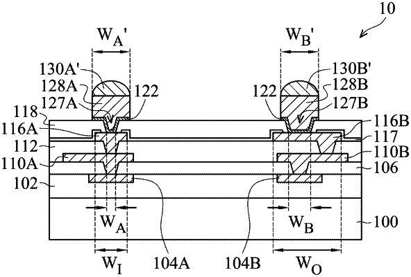
1. A semiconductor device structure, comprising:
a semiconductor substrate;
an interconnection structure over the semiconductor substrate;
a first conductive pillar over the interconnection structure, wherein the first conductive pillar has a first protruding portion extending towards the semiconductor substrate from a lower surface of the first conductive pillar; and
a second conductive pillar over the interconnection structure, wherein the second conductive pillar is substantially as wide as the first conductive pillar, the second conductive pillar has a second protruding portion extending towards the semiconductor substrate from a lower surface of the second conductive pillar, the first conductive pillar is closer to a center point of the semiconductor substrate than the second conductive pillar, a bottom of the second protruding portion is wider than a bottom of the first protruding portion, and the bottoms of the first protruding portion and the second protruding portion are substantially level with each other.
|