| CPC H01L 24/14 (2013.01) [H01L 23/5226 (2013.01); H01L 23/528 (2013.01); H01L 23/53204 (2013.01); H01L 2224/0401 (2013.01)] | 15 Claims |
|
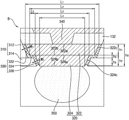
1. A semiconductor package, comprising:
a semiconductor chip;
a lower redistribution layer on a lower surface of the semiconductor chip;
a lower passivation layer on a lower surface of the lower redistribution layer;
an under bump metallization (UBM) pad on the lower passivation layer, the UBM pad including an upper pad and a lower pad connected to the upper pad, the upper pad having a greater horizontal length between outermost edges of an entire uppermost surface thereof than a horizontal length between outermost edges of an entire lowermost surface thereof, the uppermost surface vertically overlapping the lowermost surface, and the upper pad being between the lower pad and the lower redistribution layer;
a seed layer between the lower passivation layer and the UBM pad; and
an external connecting terminal on a lower surface of the UBM pad,
wherein the seed layer includes:
a first seed part covering a side surface of the upper pad,
a second seed part covering at least a portion of the lower surface of the upper pad, and
a third seed part covering at least a portion of a side surface of the lower pad.
|