| CPC H01L 24/06 (2013.01) [H01L 22/14 (2013.01); H01L 24/03 (2013.01); H01L 24/05 (2013.01); H01L 24/80 (2013.01); H01L 24/83 (2013.01); H01L 24/92 (2013.01); H01L 2224/03921 (2013.01); H01L 2224/05541 (2013.01); H01L 2224/05554 (2013.01); H01L 2224/0603 (2013.01); H01L 2224/06132 (2013.01); H01L 2224/80031 (2013.01); H01L 2224/80895 (2013.01); H01L 2224/83896 (2013.01); H01L 2224/9211 (2013.01)] | 10 Claims |
|
1. An electronic circuit comprising a surface intended to be attached to another electronic circuit by hybrid molecular bonding, the electronic circuit comprising:
an electrically-insulating layer exposed on said surface;
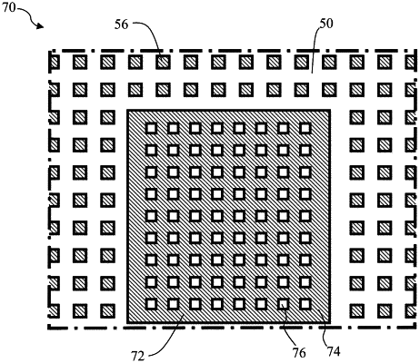
distributed in the electrically-insulating layer, first electrically-conductive bonding pads exposed on a first portion of said surface, the density of first bonding pads on the first portion of said surface being smaller than 30%; and
at least one electrically-conductive test pad, exposed on a second portion of said surface containing a square having a side length greater than 30 μm, the density of electrically-conductive material of the test pad exposed on the second portion of said surface being in the range from 40% to 80% and, everywhere in the second portion of said surface, at least one dimension of the electrically-conductive material exposed on the second portion of said surface being smaller than 10 μm.
|