| CPC H01L 24/05 (2013.01) [B81C 3/00 (2013.01); G06V 40/13 (2022.01); G06V 40/1329 (2022.01); H01L 23/053 (2013.01); H01L 24/16 (2013.01); H01L 24/32 (2013.01); H01L 24/73 (2013.01); H01L 23/3128 (2013.01); H01L 24/03 (2013.01); H01L 24/11 (2013.01); H01L 24/13 (2013.01); H01L 24/27 (2013.01); H01L 24/29 (2013.01); H01L 24/33 (2013.01); H01L 24/81 (2013.01); H01L 24/83 (2013.01); H01L 24/92 (2013.01); H01L 2224/0345 (2013.01); H01L 2224/03452 (2013.01); H01L 2224/03464 (2013.01); H01L 2224/0347 (2013.01); H01L 2224/0361 (2013.01); H01L 2224/03912 (2013.01); H01L 2224/0401 (2013.01); H01L 2224/05124 (2013.01); H01L 2224/05139 (2013.01); H01L 2224/05144 (2013.01); H01L 2224/05147 (2013.01); H01L 2224/05155 (2013.01); H01L 2224/05166 (2013.01); H01L 2224/05624 (2013.01); H01L 2224/05639 (2013.01); H01L 2224/05644 (2013.01); H01L 2224/05647 (2013.01); H01L 2224/05655 (2013.01); H01L 2224/05666 (2013.01); H01L 2224/05671 (2013.01); H01L 2224/05684 (2013.01); H01L 2224/1132 (2013.01); H01L 2224/11334 (2013.01); H01L 2224/1146 (2013.01); H01L 2224/1147 (2013.01); H01L 2224/11849 (2013.01); H01L 2224/119 (2013.01); H01L 2224/13013 (2013.01); H01L 2224/13014 (2013.01); H01L 2224/131 (2013.01); H01L 2224/13111 (2013.01); H01L 2224/13147 (2013.01); H01L 2224/13294 (2013.01); H01L 2224/133 (2013.01); H01L 2224/16227 (2013.01); H01L 2224/27312 (2013.01); H01L 2224/2732 (2013.01); H01L 2224/27622 (2013.01); H01L 2224/2784 (2013.01); H01L 2224/29006 (2013.01); H01L 2224/29007 (2013.01); H01L 2224/29011 (2013.01); H01L 2224/2919 (2013.01); H01L 2224/2929 (2013.01); H01L 2224/29294 (2013.01); H01L 2224/29299 (2013.01); H01L 2224/2939 (2013.01); H01L 2224/32225 (2013.01); H01L 2224/33181 (2013.01); H01L 2224/73204 (2013.01); H01L 2224/73253 (2013.01); H01L 2224/81191 (2013.01); H01L 2224/81203 (2013.01); H01L 2224/81424 (2013.01); H01L 2224/81439 (2013.01); H01L 2224/81444 (2013.01); H01L 2224/81447 (2013.01); H01L 2224/81455 (2013.01); H01L 2224/8146 (2013.01); H01L 2224/81464 (2013.01); H01L 2224/81466 (2013.01); H01L 2224/81471 (2013.01); H01L 2224/81484 (2013.01); H01L 2224/81815 (2013.01); H01L 2224/8185 (2013.01); H01L 2224/83101 (2013.01); H01L 2224/83102 (2013.01); H01L 2224/83192 (2013.01); H01L 2224/9211 (2013.01); H01L 2224/92125 (2013.01); H01L 2224/92225 (2013.01); H01L 2924/014 (2013.01); H01L 2924/1815 (2013.01); H01L 2924/18161 (2013.01)] | 18 Claims |
|
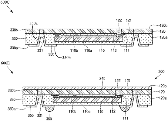
1. A fingerprint sensor device comprising:
a substrate comprising:
an upper substrate side, a bottom substrate side, and lateral substrate sides between the upper and bottom substrate sides;
a dielectric layer having an upper dielectric layer side, a lower dielectric layer side, and a lateral dielectric side extending between the upper dielectric layer side and the lower dielectric layer side; and
a conductive layer exposed from the upper dielectric layer side and the lower dielectric layer side;
a semiconductor die having a top die side facing the bottom substrate side, a bottom die side, and lateral die sides between the top and bottom die sides;
a plurality of first conductive interconnection structures electrically connecting the top die side to the bottom substrate side;
protective material adhered directly to the top die side and the bottom substrate side; and
a protective layer on the upper substrate side,
wherein:
the protective material does not contact the protective layer, and
the fingerprint sensor device is configured to sense a fingerprint of a finger positioned above the top die side.
|