| CPC H01L 24/05 (2013.01) [H01L 23/49822 (2013.01); H01L 23/49844 (2013.01); H01L 24/03 (2013.01); H01L 25/0657 (2013.01); H01L 2224/03001 (2013.01); H01L 2224/033 (2013.01); H01L 2224/05556 (2013.01); H01L 2224/05573 (2013.01)] | 20 Claims |
|
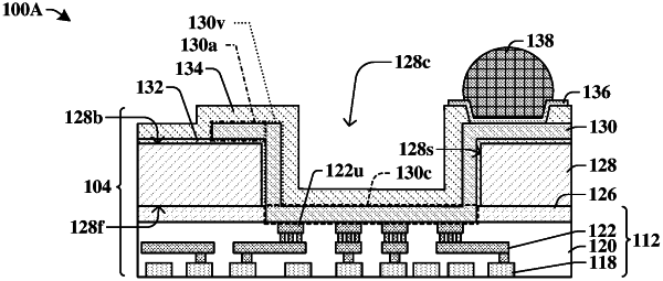
1. A device comprising:
a substrate;
an interconnect structure arranged on a frontside of the substrate and comprising multiple interconnect conductive structures embedded within an interconnect dielectric structure;
a bonding structure arranged on a backside of the substrate; a bond pad structure arranged on the backside of the substrate and extending completely through the substrate to contact the multiple interconnect conductive structures, wherein the bond pad structure comprises:
a backside horizontal portion arranged on the backside of the substrate and directly below the bonding structure;
a vertical portion arranged on inner sidewalls of the substrate; and
a frontside horizontal portion arranged over the multiple interconnect conductive structures; and
a barrier layer arranged directly between the bond pad structure and the multiple interconnect conductive structures.
|