| CPC H01L 24/05 (2013.01) [H01L 21/78 (2013.01); H01L 24/03 (2013.01); H01L 2224/03462 (2013.01); H01L 2224/04042 (2013.01); H01L 2224/05022 (2013.01); H01L 2224/05026 (2013.01); H01L 2224/05118 (2013.01); H01L 2224/05147 (2013.01); H01L 2224/05155 (2013.01); H01L 2224/05171 (2013.01); H01L 2224/05568 (2013.01)] | 10 Claims |
|
1. A semiconductor package device, comprising:
a chip comprising:
a chip substrate having a front surface and a back surface, wherein the front surface includes a photosensitive region;
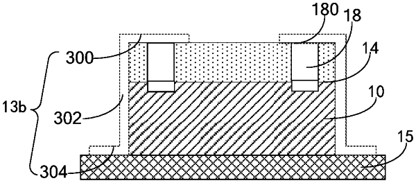
soldering pads disposed at the front surface of the chip substrate surrounding the photosensitive region;
a metal part formed on a side of each soldering pad facing away from the chip substrate; and
a transparent protective layer formed on the front surface of the chip substrate, wherein the transparent protective layer covers the photosensitive region of the chip substrate;
a circuit board, on the back surface of the chip substrate; and
a conductive connection part including a first portion and a second portion, wherein
the first portion is in parallel with the front surface of the chip substrate and electrically connects to the metal part,
the second portion is disposed on a sidewall of the transparent protective layer and on a sidewall of the chip substrate, and an end part of the second portion is physically and electrically connected to the circuit board, and
the chip and the circuit board are electrically connected with each other.
|