| CPC H01L 24/03 (2013.01) [H01L 24/02 (2013.01); H01L 24/94 (2013.01); H01L 24/05 (2013.01); H01L 2224/02206 (2013.01); H01L 2224/0221 (2013.01); H01L 2224/02215 (2013.01); H01L 2224/03019 (2013.01); H01L 2224/03614 (2013.01); H01L 2224/03622 (2013.01); H01L 2224/03632 (2013.01); H01L 2224/05624 (2013.01); H01L 2224/05647 (2013.01)] | 17 Claims |
|
1. A semiconductor structure, comprising:
a semiconductor wafer with a wafer active surface, wherein a plurality of contact pads are formed on the wafer active surface;
an insulating layer disposed on the wafer active surface to cover the wafer active surface and the contact pads;
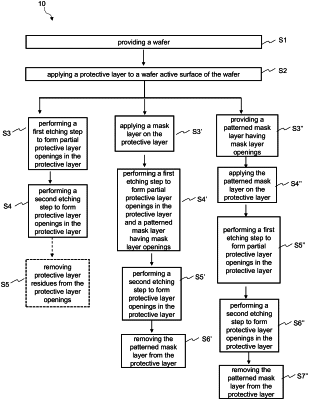
a mask layer disposed on the insulating layer, wherein a plurality of mask layer openings are formed in the mask layer in a multi-step etching process to expose top portions of the insulating layer corresponding to the contact pads from the mask layer; and
a plurality of via openings configured to expose the contact pads, the via openings being formed in the insulating layer by removing the top portions of the insulating layer from the mask layer openings corresponding to the contact pads in the multi-step etching process, wherein forming the via openings comprises forming partial via opening before a final etching step of the multi-step etching process by leaving a remaining insulating layer in the via openings.
|