| CPC H01L 24/03 (2013.01) [H01L 24/05 (2013.01); H01L 24/27 (2013.01); H01L 24/29 (2013.01); H01L 24/08 (2013.01); H01L 24/32 (2013.01); H01L 2224/03013 (2013.01); H01L 2224/0345 (2013.01); H01L 2224/03462 (2013.01); H01L 2224/03464 (2013.01); H01L 2224/0355 (2013.01); H01L 2224/03612 (2013.01); H01L 2224/03622 (2013.01); H01L 2224/0381 (2013.01); H01L 2224/05083 (2013.01); H01L 2224/05084 (2013.01); H01L 2224/05546 (2013.01); H01L 2224/05564 (2013.01); H01L 2224/08145 (2013.01); H01L 2224/08225 (2013.01); H01L 2224/2781 (2013.01); H01L 2224/27831 (2013.01); H01L 2224/29006 (2013.01); H01L 2224/29027 (2013.01); H01L 2224/29028 (2013.01); H01L 2224/32145 (2013.01); H01L 2224/32225 (2013.01)] | 19 Claims |
|
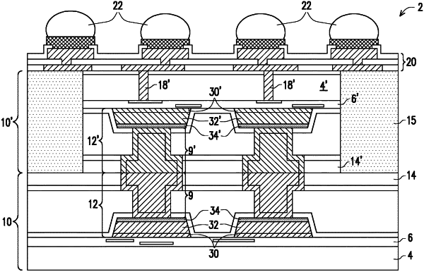
1. A method comprising:
forming a conductive pad over an interconnect structure of a wafer;
forming a capping layer over the conductive pad;
forming an anti-reflective coating over the capping layer;
depositing a dielectric layer over the anti-reflective coating;
etching the dielectric layer to form an opening in the dielectric layer, wherein the capping layer is exposed to the opening;
performing a wet-cleaning process on the wafer, wherein during the wet-cleaning process, a top surface of the capping layer is exposed to a chemical solution used for performing the wet-cleaning process;
depositing a conductive diffusion barrier extending into the opening and penetrating through the anti-reflective coating; and
depositing a conductive material over the conductive diffusion barrier.
|