| CPC H01L 23/562 (2013.01) [H01L 21/4853 (2013.01); H01L 21/4857 (2013.01); H01L 21/565 (2013.01); H01L 21/568 (2013.01); H01L 23/3121 (2013.01); H01L 23/5383 (2013.01); H01L 23/5386 (2013.01); H01L 23/5389 (2013.01); H01L 24/19 (2013.01); H01L 24/20 (2013.01); H01L 2224/214 (2013.01); H01L 2924/3511 (2013.01)] | 15 Claims |
|
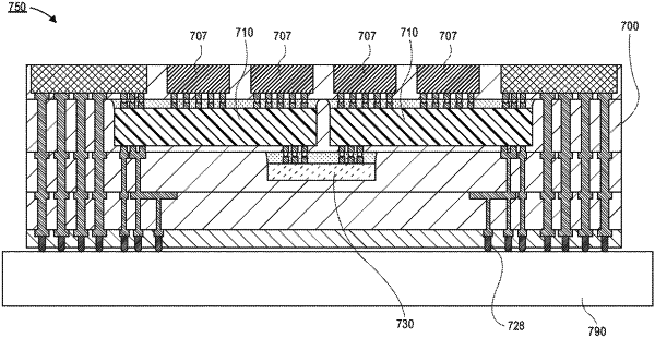
1. A multi-die electronic package, comprising:
a first die in a first mold layer, the first die comprising interconnections;
a first via and a second via in the first mold layer, the first via and the second via laterally adjacent to a first side of the first die, the first side laterally opposite a second side, each of the first via and the second via extending from a top surface of the first mold layer to a bottom surface of the first mold layer;
a third via and a fourth via in the first mold layer, each of the third via and the fourth via extending from the top surface of the first mold layer to the bottom surface of the first mold layer;
a second die electrically coupled to the first die, and the second die electrically coupled to the first via and the second via;
a third die electrically coupled to the first die, the third die electrically coupled to the second die by the interconnections of the first die;
a fourth die in the first mold layer, the fourth die laterally spaced apart from the first die, the fourth die having a first side facing toward the second side of the first die, and the fourth die having a second side laterally opposite the first side, wherein the third via and the fourth via are laterally adjacent to the second side of the fourth die;
a fifth die laterally spaced apart from the third die, the fifth die electrically coupled to the fourth die, and the fifth die electrically coupled to the third via and the fourth via; and
a second mold layer between and in contact with the second die and the third die, the second mold layer between and in contact with the third die and the fifth die, the second mold layer having an upper surface co-planar with an upper surface of the third die, the second mold layer between the second die and the first die, and the second mold layer between the third die and the first die.
|