| CPC H01L 23/562 (2013.01) [H01L 21/76898 (2013.01); H01L 23/481 (2013.01)] | 16 Claims |
|
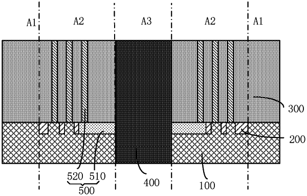
1. A semiconductor structure, wherein the semiconductor structure is provided with a first area, a second area and a third area, the second area being arranged between the first area and the third area, the semiconductor structure comprising:
a substrate;
a shallow trench isolation structure arranged in the substrate and configured to isolate the substrate into a plurality of active areas, the active areas in the first area forming a semiconductor device;
a dielectric layer arranged on the substrate;
a through hole structure arranged in the third area, the through hole structure penetrating through the dielectric layer and the substrate; and
a stress buffer structure arranged in the second area, the stress buffer structure comprising a first buffer doped area, the first buffer doped area being arranged in the active areas and formed by doping the active areas with a first buffer impurity, an atomic radius of the first buffer impurity being less than an atomic radius of a material of the substrate;
wherein the stress buffer structure further comprises at least one buffer window structure arranged in the dielectric layer, there is a spacing between the buffer window structure and the through hole structure, the buffer window structure comprises a buffer through hole structure, and a buffer through hole of the buffer through hole structure is filled with a metal plug;
wherein the buffer window structure is grounded; or wherein a second end of the at least one buffer window structure is connected to the active areas; or wherein a second end of the at least one buffer window structure is connected to the first buffer doped area.
|