| CPC H01L 23/562 (2013.01) [H01L 21/31144 (2013.01); H01L 21/76224 (2013.01); H01L 22/12 (2013.01)] | 20 Claims |
|
1. A method for fabricating a plurality of semiconductor devices in a semiconductor wafer, the method comprising:
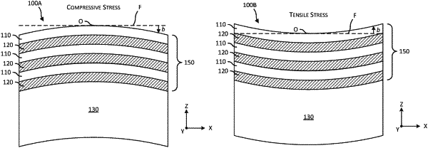
bowing the semiconductor wafer comprising a substrate by covering the substrate with a strained layer;
forming trenches through the strained layer into the substrate at locations in scribe lines of the semiconductor wafer, respective bottoms of the trenches being located in the substrate below the strained layer, the scribe lines identifying areas between adjacent dies on the semiconductor wafer; and
reducing the bowing of the semiconductor wafer by filling the trenches with a stress-compensation material.
|