| CPC H01L 23/552 (2013.01) [H01L 21/56 (2013.01); H01L 21/561 (2013.01); H01L 21/568 (2013.01); H01L 23/49822 (2013.01)] | 22 Claims |
|
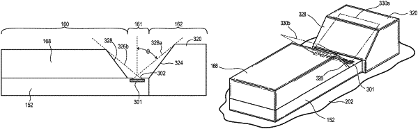
1. A method of making a semiconductor device, comprising:
providing a semiconductor package including a substrate and an encapsulant deposited over a first portion of the substrate, wherein the encapsulant includes a sloped surface oriented toward a second portion of the substrate;
disposing a mask over the second portion of the substrate, wherein the mask includes a sloped surface oriented toward the encapsulant, and wherein an area between the sloped surface of the encapsulant and the sloped surface of the mask remains devoid of the encapsulant;
forming a shielding layer over the semiconductor package and mask; and
removing the mask after forming the shielding layer.
|