| CPC H01L 23/552 (2013.01) [H01L 23/49861 (2013.01); H01L 23/645 (2013.01); H01L 24/16 (2013.01); H01L 24/48 (2013.01); H01L 2224/16221 (2013.01); H01L 2224/48249 (2013.01); H01L 2224/48257 (2013.01); H01L 2924/182 (2013.01); H01L 2924/3025 (2013.01)] | 20 Claims |
|
1. A semiconductor package with an integrated and shielded lead-frame inductor comprising:
a semiconductor chip having transistors formed in a semiconductor material and having integrated wiring integrated together on a chip substrate;
chip bonding pads connected to the integrated wiring and formed on a perimeter of the chip substrate;
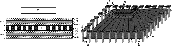
an inductor coil having an air core, the inductor coil being a planar inductor that is substantially in a plane of the inductor coil, the plane of the inductor coil being parallel to a plane of the semiconductor chip;
an upper ferrite-dielectric shield having a ferrite layer and a dielectric layer above the ferrite layer and a dielectric layer below the ferrite layer, the inductor coil being electrically isolated from the ferrite layer by the dielectric layer;
wherein the upper ferrite-dielectric shield is in a plane parallel to and between the plane of the inductor coil and the plane of the semiconductor chip;
a plurality of lead-frame pads placed around a perimeter of the inductor coil and surrounding the semiconductor chip;
bonding wires that connect the chip bonding pads on the semiconductor chip to the plurality of lead-frame pads;
a plurality of lead-frame risers that connect the plurality of lead-frame pads to package pins for electrically connecting to an external system;
a center post that connects to an inner end of the inductor coil and is electrically connected to the semiconductor chip; and
a lead-frame outer riser that connects an outer end of the inductor coil to a package pin for electrically connecting to the external system.
|