| CPC H01L 23/552 (2013.01) [H01L 23/31 (2013.01); H05K 9/0045 (2013.01); H05K 9/0081 (2013.01)] | 5 Claims |
|
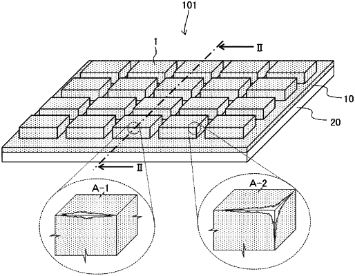
1. An electromagnetic wave shielding sheet before thermal pressing for forming an electromagnetic wave shielding layer, used for an electronic component-mounting substrate comprising a substrate, an electronic component mounted on one or both surfaces of the substrate, and an electromagnetic wave shielding layer that covers a step part formed by mounting the electronic component and at least a part of an exposed surface of the substrate and includes at least one of an electromagnetic wave reflection layer and an electromagnetic wave absorption layer, wherein:
the electromagnetic wave shielding sheet includes at least one of a conductive layer before thermal pressing of the electromagnetic wave reflection layer and a conductive layer before thermal pressing of the electromagnetic wave absorption layer;
the conductive layer before thermal pressing of the electromagnetic wave reflection layer comprises a binder resin and a conductive filler;
the conductive layer before thermal pressing of the electromagnetic wave absorption layer comprises a binder resin and an electromagnetic wave absorption filler; and
a Young's modulus of the conductive layer at 23° C. is 10 to 700 MPa.
|