| CPC H01L 23/544 (2013.01) [H01L 23/49838 (2013.01); H01L 24/73 (2013.01); H04L 9/3278 (2013.01); H01L 2223/54413 (2013.01); H01L 2224/73204 (2013.01)] | 19 Claims |
|
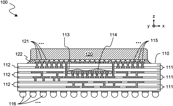
1. An integrated circuit (IC) package substrate comprising:
an insulator layer;
a physical unclonable function (PUF) structure, the PUF structure comprising:
a level of metallization comprising an array of electrodes at a side of the insulator layer; and
a cap layer over the array, the cap layer in contact with individual ones of the electrodes and in contact with at least a portion of the insulator layer between adjacent ones of the electrodes, wherein the cap layer comprises a material having a different composition or microstructure than the metallization, wherein the material is a first material which forms first microstructures of the cap layer, wherein second microstructures formed by the cap layer are each located between respective ones of the first microstructures, wherein the second microstructures each comprise a respective void or a second material other than the first material; and
a dielectric material over the PUF structure.
|