| CPC H01L 23/5384 (2013.01) [H01L 21/486 (2013.01); H01L 21/60 (2021.08); H01L 21/76802 (2013.01); H01L 24/80 (2013.01); H01L 25/0655 (2013.01)] | 20 Claims |
|
1. A method for forming a chip package structure, comprising:
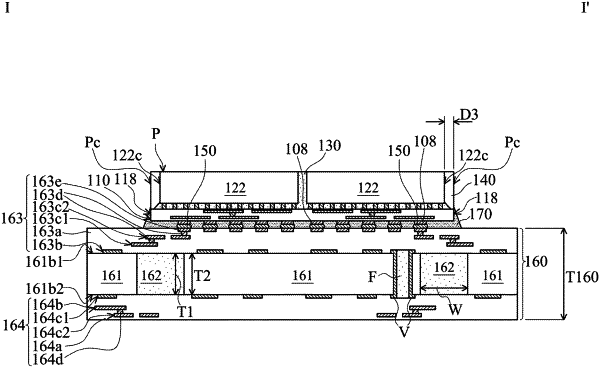
removing a first portion of a substrate to form a first recess in the substrate;
forming a buffer structure in the first recess, wherein a first Young's modulus of the buffer structure is less than a second Young's modulus of the substrate;
forming a first wiring structure over the buffer structure and the substrate, wherein the first wiring structure comprises a first dielectric structure and a first wiring layer in the first dielectric structure; and
bonding a chip package to the first wiring structure, wherein the chip package has an interposer substrate and a chip structure over the interposer substrate, and a first corner of the interposer substrate and a second corner of the chip structure overlap the buffer structure in a top view of the chip package and the buffer structure.
|