| CPC H01L 23/535 (2013.01) [H01L 23/53257 (2013.01); H10B 41/27 (2023.02); H10B 43/27 (2023.02)] | 10 Claims |
|
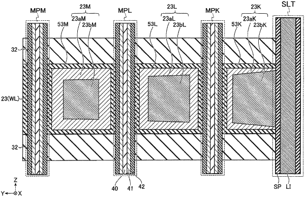
1. A semiconductor memory device comprising:
a first insulating layer;
a first conductive layer provided above the first insulating layer and containing tungsten, the first conductive layer including a first sub conductive layer and a second sub conductive layer;
a first pillar that passes through the first insulating layer and the first conductive layer and extends in a first direction;
a second pillar that passes through the first insulating layer and the first conductive layer and extends in the first direction; and
a second insulating layer that extends in a second direction and divides the first insulating layer and the first conductive layer, the second direction intersecting with the first direction, wherein
the first pillar is located between the second insulating layer and the second pillar with respect to a third direction that intersects the first direction and the second direction,
the first sub conductive layer is in contact with the second sub conductive layer and is provided between the second sub conductive layer and the first insulating layer,
a fluorine concentration in the first sub conductive layer is lower than that in the second sub conductive layer,
the first sub conductive layer includes a first portion located between the second insulating layer and the first pillar and a second portion located between the first pillar and the second pillar, and
a thickness of the first sub conductive layer in the first portion is smaller than that of the first sub conductive layer in the second portion.
|