| CPC H01L 23/53266 (2013.01) [H01L 21/7684 (2013.01); H01L 21/76843 (2013.01); H01L 21/76877 (2013.01); H01L 23/5226 (2013.01)] | 12 Claims |
|
1. A method for forming a semiconductor device, comprising:
providing a base;
forming an interlayer dielectric layer over the base;
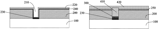
forming a contact hole by etching the interlayer dielectric layer, the contact hole exposing a portion of a surface of the base;
forming a reactive metal layer at a bottom and on a sidewall of the contact hole and over the interlayer dielectric layer;
forming a diffusion barrier layer over the reactive metal layer;
after forming the diffusion barrier layer over the reactive metal layer, forming a silicide layer by reacting a portion of the reactive metal layer at the bottom of the contact hole with a portion of a surface of the base;
removing the diffusion barrier layer and a remaining portion of the metal layer that is unreacted;
after removing the diffusion barrier layer and the remaining portion of the metal layer that is unreacted, forming a barrier layer over the base in the contact hole; and
forming a metal layer over the barrier layer and fully filling the contact hole, including:
forming a first metal layer in the contact hole;
forming a second metal layer on the first metal layer; and
after forming the first metal layer and before forming the second metal layer, forming an adhesion layer on the interlayer dielectric layer.
|