| CPC H01L 23/53219 (2013.01) [H01L 21/76802 (2013.01); H01L 21/76877 (2013.01); H01L 21/76888 (2013.01); H01L 23/5226 (2013.01); H01L 23/53223 (2013.01); H10B 41/27 (2023.02); H10B 43/27 (2023.02)] | 10 Claims |
|
1. A three-dimensional memory device, comprising:
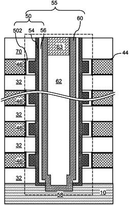
an alternating stack of insulating layers and electrically conductive layers located over a substrate, wherein the electrically conductive layers comprise an intermetallic alloy of aluminum and at least one metal other than aluminum;
memory openings vertically extending through the alternating stack;
memory opening fill structures located in a respective one of the memory openings and comprising a respective vertical semiconductor channel and a respective vertical stack of memory elements; and
an insulating spacer having a lengthwise sidewall that laterally extends along a first horizontal direction and contacting a sidewall of each of the insulating layers and the electrically conductive layers,
wherein each of the electrically conductive layers has a lateral compositional gradient such that an atomic concentration of aluminum increases with a lateral distance from a most proximal one of the memory opening fill structures; and
wherein a maximum atomic concentration of aluminum within the electrically conductive layers is located at or in proximity to an interface with the insulating spacer.
|