| CPC H01L 23/5286 (2013.01) [H01L 21/31116 (2013.01); H01L 21/76816 (2013.01); H01L 21/76829 (2013.01); H01L 23/5226 (2013.01); H01L 23/5283 (2013.01); H01L 21/823871 (2013.01); H01L 27/092 (2013.01); H01L 29/0665 (2013.01); H01L 29/42392 (2013.01)] | 6 Claims |
|
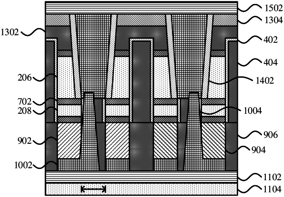
1. An integrated chip, comprising:
a frontside device above a base layer, having a channel and source/drain structures;
a buried power rail in the base layer, underneath the frontside device; and
an electrical contact that makes an electrical connection between the buried power rail and the frontside device,
wherein the base layer includes:
a first etch stop layer, which the buried power rail penetrates;
a first semiconductor layer between the first etch stop layer and the frontside device;
a second etch stop layer, between the first semiconductor layer and the frontside device;
a second semiconductor layer between the second etch stop layer and the frontside device; and
a third etch stop layer between the second semiconductor layer and the frontside device.
|
|
4. An integrated chip, comprising:
a plurality of frontside devices above a base layer, each having a channel and source/drain structures, and having an inter-device distance between an adjacent pair of frontside devices of the plurality of frontside devices;
a buried power rail in the base layer, underneath the pair of frontside devices, having a width that is greater than the inter-device distance; and
an electrical contact that makes an electrical connection between the buried power rail and one of the pair of frontside devices,
wherein the base layer includes:
a first etch stop laver, which the buried power rail penetrates;
a first semiconductor layer between the first etch stop layer and the one of the pair of frontside devices;
a second etch stop layer, between the first semiconductor layer and the one of the pair of frontside devices;
a second semiconductor layer between the second etch stop layer and the one of the pair of frontside devices; and
a third etch stop layer between the second semiconductor layer and the one of the pair of frontside devices.
|