| CPC H01L 23/5283 (2013.01) [H01L 21/563 (2013.01); H01L 21/565 (2013.01); H01L 23/3114 (2013.01); H01L 23/3128 (2013.01); H01L 24/09 (2013.01); H01L 24/17 (2013.01); H01L 2224/0231 (2013.01); H01L 2224/02373 (2013.01); H01L 2224/02381 (2013.01); H01L 2224/0401 (2013.01)] | 21 Claims |

|
1. A method to manufacture a semiconductor device, comprising:
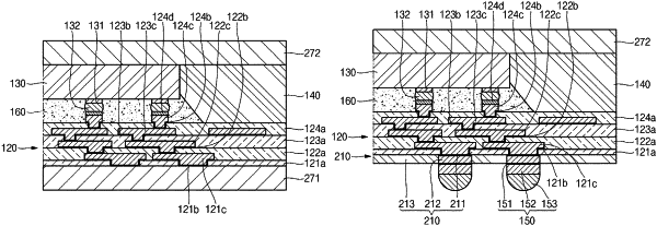
providing a redistribution layer (RDL) substrate on a first carrier, the RDL substrate having a top surface, a bottom surface, and a conductive structure;
placing an electronic device on the top surface of the RDL substrate;
providing a first protective material using a first molding operation, wherein the first protective material covers a side surface of the electronic device and the top surface of the RDL substrate;
attaching a second carrier to the first protective material;
removing the first carrier from the RDL substrate to expose the bottom surface of the RDL substrate and the conductive structure;
providing a conductive post on the bottom surface of the RDL substrate using a first plating operation;
providing a base structure comprising a second protective material using a second molding operation, wherein the second protective material covers a side surface of the conductive post and the bottom surface of the RDL substrate;
providing a base layer on a bottom side of the conductive post, wherein a bottommost side of the base layer is at a bottommost side of the second protective material; and
providing a conductive pillar below a bottom side of the base structure and coupled with the conductive post, wherein the conductive pillar is coupled with the conductive post through an opening in the base structure.
|