| CPC H01L 23/5283 (2013.01) [H01L 21/76816 (2013.01); H01L 21/76829 (2013.01); H01L 21/76877 (2013.01); H01L 23/5226 (2013.01)] | 20 Claims |
|
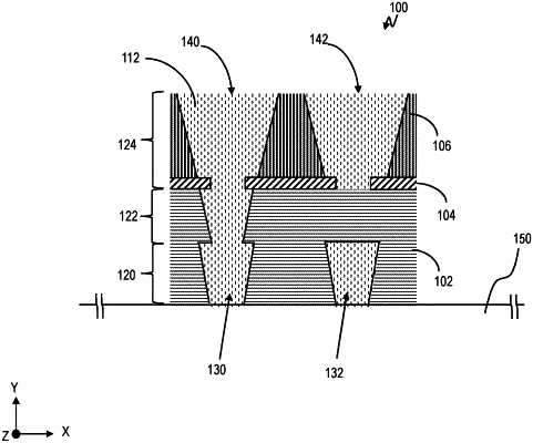
1. An integrated circuit (IC) comprising:
a conductive line formed on a conductive via, the conductive line being formed though a dielectric material; and
an etch stop layer comprising one or more extended portions intervening between one or more edge portions of the conductive line and the conductive via, the one or more edge portions being at a periphery of the conductive line and the conductive via, the etch stop layer comprising a higher dielectric breakdown than the dielectric material, the one or more extended portions of the etch stop layer causing the conductive line to be formed with a bottom part having a reduced dimension than an upper part of the conductive line, a bottom surface of the upper part in direct contact with a top surface of the one or more extended portions of the etch stop layer.
|
|
11. An integrated circuit (IC) comprising:
a conductive via formed in a first dielectric material;
a dielectric layer formed on the conductive via and the first dielectric material; and
a conductive line comprising an upper part and a bottom part, the dielectric layer comprising one or more extended portions intervening between one or more edge portions of the conductive line and the conductive via, the one or more edge portions being at a periphery of the conductive line and the conductive via, the dielectric layer being formed to have an opening to the conductive via, the bottom part being formed on the conductive via through the opening, the upper part being formed through a second dielectric material above the dielectric layer, a bottom surface of the upper part in direct contact with a top surface of the one or more extended portions of the dielectric layer.
|