| CPC H01L 23/5283 (2013.01) [H01L 21/76877 (2013.01); H01L 23/5226 (2013.01); H01L 23/528 (2013.01)] | 14 Claims |
|
1. A semiconductor device comprising a front-end-of-line (FEOL) structure and a back-end-of-line (BEOL) structure connected to the FEOL structure,
wherein the FEOL structure comprises at least one source/drain region and at least one gate structure, and
wherein the BEOL structure comprises:
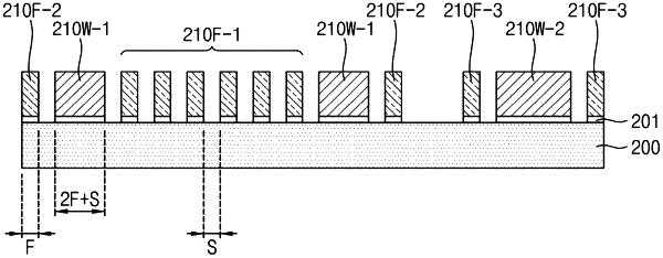
a plurality of 1st fine metal lines arranged in a row at a same pitch, each of the plurality of 1st fine metal lines having a same width;
at least one 1st wide metal line formed at a side of the plurality of 1st fine metal lines, the 1st wide metal line having a width greater than the width of the 1st fine metal line;
a 2nd fine metal line at a side of the 1st wide metal line opposite to the 1st fine metal lines; and
a 3rd fine metal line at a side of the 2nd fine metal line opposite to the 1st wide metal line,
wherein no other metal lines are present between the 2nd fine metal line and the 3rd fine metal line at a same level,
wherein a width of a space between the 2nd fine metal line and the 3rd fine metal line is greater than the width of the space between the two adjacent 1st fine metal lines, and
wherein each of the plurality of 1st fine metal lines comprises a material different from a material included in the 1st wide metal line.
|