| CPC H01L 23/5283 (2013.01) [H01L 23/5226 (2013.01); H01L 23/552 (2013.01); H01L 23/562 (2013.01); H01L 24/16 (2013.01); H01L 24/94 (2013.01); H01L 2224/16227 (2013.01)] | 16 Claims |
|
1. An electronic package, comprising:
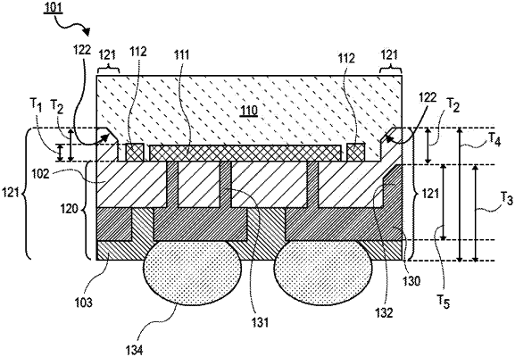
a redistribution layer (RDL) over a package substrate, wherein the RDL comprises:
a conductive layer in a first dielectric layer, the first dielectric layer having a lateral width;
a second dielectric layer over the conductive layer and the first dielectric layer; and
an extended portion of the RDL having a first thickness, wherein the first thickness vertically extends from a bottom surface of the first dielectric layer to a topmost surface of the second dielectric layer; and
a die on the RDL, wherein the die has a plurality of sidewall surfaces, a top surface, and a bottom surface that is opposite from the top surface, the die having a trench-shaped region with a tapered sidewall profile joining a vertical portion and a horizontal portion at one of the sidewall surfaces, and the die having a lateral width the same as the lateral width of the first dielectric layer, wherein the die has an active region that is located on the bottom surface of the die, wherein the RDL electrically couples the active region to the package substrate, wherein the first thickness is greater than a second thickness of the RDL that vertically extends from the bottom surface of the first dielectric layer to the bottom surface of the die, and wherein the extended portion is over and around a first region of the bottom surface of the die and a second region of the sidewall surfaces of the die including in the trench-shaped region and on the tapered sidewall profile, on the vertical portion and on the horizontal portion at the one of the sidewall surfaces.
|