| CPC H01L 23/528 (2013.01) [H01L 23/5226 (2013.01); H01L 27/0207 (2013.01)] | 14 Claims |
|
1. A semiconductor device comprising:
a first circuit;
a second circuit;
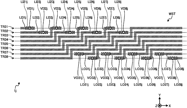
a wiring structure connected to the first circuit and the second circuit, the wiring structure including:
a first outer track extending in a first direction;
a second outer track extending in the first direction;
a plurality of inner tracks which are disposed between the first outer track and the second outer track and extending in the first direction; and
a plurality of wirings, each of which has a stepwise pattern at the inner tracks or extends obliquely with respect to the inner tracks, and has an end portion at the first outer track or the second outer track, wherein
the plurality of wirings includes a first line laid out along the first outer track and having an end portion that is laid out along the second outer track and a second line laid out along the second outer track and having an end portion that is laid out along the first outer track.
|