| CPC H01L 23/528 (2013.01) [H01L 21/31144 (2013.01); H01L 21/76802 (2013.01); H01L 21/76816 (2013.01); H01L 21/76877 (2013.01); H01L 23/48 (2013.01); H01L 23/522 (2013.01); H01L 27/0207 (2013.01); H10B 41/10 (2023.02); H10B 41/40 (2023.02); H10B 41/41 (2023.02); H01L 2924/0002 (2013.01)] | 17 Claims |
|
1. A semiconductor device comprising:
a semiconductor substrate extending in a first direction, a second direction, and a third direction, the first to third directions crossing one another, the semiconductor substrate having a front surface at a first side in the third direction and a rear surface at a second side in the third direction, the first surface having patterns having different heights in the third direction, the rear surface having a planar shape extending in the first direction and the second direction;
a first functioning area including a first switching element and a first conductive line, the first conductive line extending in the first direction;
a second functioning area including a second switching element and a second conductive line, the second conductive line extending in the first direction, the first conductive line and the second conductive line being provided in an imaginary plane crossing the third direction;
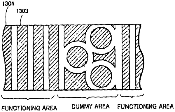
a dummy area formed on the front surface of the semiconductor substrate between the first conductive line and the second conductive line in the second direction, and being electrically isolated from the first conductive line and the second conductive line,
the dummy area including first to seventh conductive patterns physically divided in the imaginary plane,
the first, second, and third conductive patterns being arranged in this order along a fourth direction which is neither parallel nor orthogonal to the first direction,
the fourth, second, and fifth conductive patterns being arranged in this order along a fifth direction which is different from the fourth direction,
the sixth, second, and fourth seventh conductive patterns being arranged in this order along a sixth direction which is different from the fourth direction and the fifth direction.
|