| CPC H01L 23/528 (2013.01) [H01L 23/53214 (2013.01); H01L 23/53228 (2013.01); H01L 24/08 (2013.01); H01L 24/32 (2013.01); H01L 25/0657 (2013.01); H01L 2224/04026 (2013.01); H01L 2224/0807 (2013.01); H01L 2224/32145 (2013.01)] | 6 Claims |
|
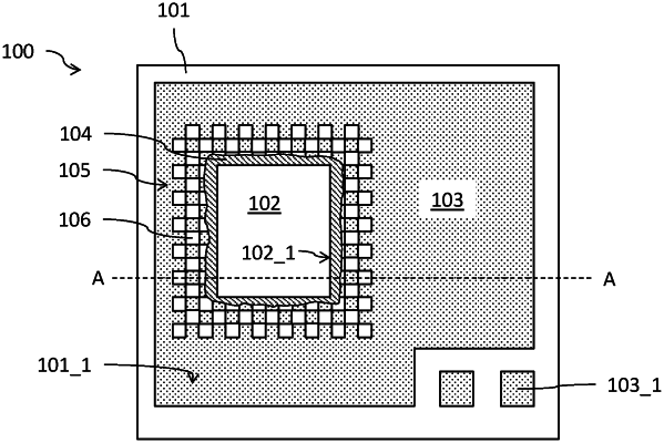
1. A method for producing a semiconductor arrangement, the method comprising:
applying a metallization layer on an upper main side of a lower semiconductor chip, structuring the metallization layer; and
fastening an upper semiconductor chip on the upper main side of the lower semiconductor chip by a bonding material,
wherein the metallization layer is structured such that the metallization layer has an increased roughness along a contour of the upper semiconductor chip in comparison with the rest of the metallization layer,
wherein wetting of the upper main side of the lower semiconductor chip by the bonding material is limited by a structure in the metallization layer to a region below the upper semiconductor chip.
|