| CPC H01L 23/528 (2013.01) [H01L 21/76807 (2013.01); H01L 21/76816 (2013.01); H01L 21/76831 (2013.01); H01L 21/76832 (2013.01); H01L 21/76834 (2013.01); H01L 21/76897 (2013.01); H01L 23/5226 (2013.01)] | 6 Claims |
|
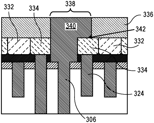
1. A semiconductor structure, comprising:
a substrate;
a plurality of alternating first and second conductive line types disposed along a same direction of a back end of line (BEOL) metallization layer disposed in an inter-layer dielectric (ILD) layer disposed above the substrate, the first conductive line type having a different composition than the second conductive line type;
a first hardmask layer disposed over the first conductive line types but not over the second conductive line types, wherein the first hardmask layer is vertically separated from the first conductive line types by a dielectric cap layer; and
a second hardmask layer disposed over the second conductive line types but not over the first conductive line types, wherein the second hardmask layer is directly on the second conductive line types, and wherein the first and second hardmask layers differ in composition.
|