| CPC H01L 23/5226 (2013.01) [H01L 27/14627 (2013.01); H01L 27/14636 (2013.01)] | 14 Claims |
|
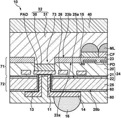
1. A semiconductor apparatus, comprising:
a first substrate, which includes a photoelectric conversion element;
an insulating member;
a second substrate overlapped with the first substrate via the insulating member; and
an electrode portion disposed between the first substrate and the second substrate,
wherein:
a through via is disposed to pass through the second substrate, and
an opening for exposing the electrode portion to outside is arranged at a position overlapping the electrode portion, and is arranged in the first substrate.
|