| CPC H01L 23/5223 (2013.01) [H01L 28/75 (2013.01); H01L 28/86 (2013.01); H01L 28/90 (2013.01)] | 20 Claims |

|
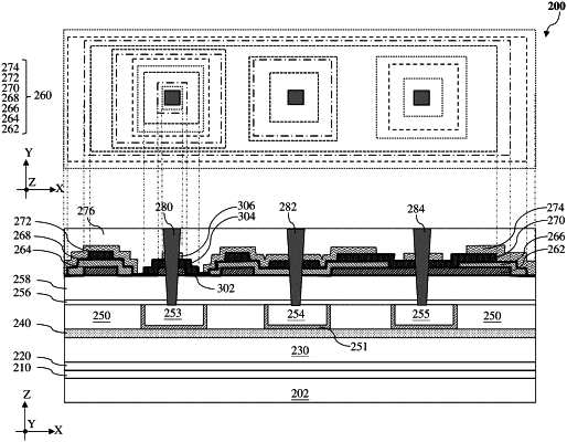
1. A device structure, comprising:
a passivation layer;
a first conductor plate layer disposed on the passivation layer;
a first dummy pad spaced apart from the first conductor plate layer by a spacing;
a second conductor plate layer disposed over the first conductor plate layer;
a third conductor plate layer disposed over the second conductor plate layer;
a second dummy pad spaced apart from the third conductor plate layer by the spacing;
a fourth conductor plate layer disposed over the third conductor plate layer; and
a third dummy pad spaced apart from the fourth conductor plate layer by the spacing,
wherein the second conductor plate layer encloses the first conductor plate layer,
wherein the fourth conductor plate layer encloses the third conductor plate layer.
|
|
12. A device structure, comprising:
a passivation layer;
a first conductor plate layer disposed on the passivation layer;
a first dummy pad spaced apart from the first conductor plate layer by a spacing;
a second conductor plate layer disposed over the first conductor plate layer;
a third conductor plate layer disposed over the second conductor plate layer;
a second dummy pad spaced apart from the third conductor plate layer by the spacing;
a fourth conductor plate layer disposed over the third conductor plate layer; and
a third dummy pad spaced apart from the fourth conductor plate layer by the spacing,
wherein, along a direction, the first conductor plate layer comprises a first width, the second conductor plate layer comprises a second width, the third conductor plate layer comprises a third width, and the fourth conductor plate layer comprises a fourth width,
wherein the second width is greater than the first width and the fourth width is greater than the third width.
|
|
17. A device structure, comprising:
a passivation layer;
a first conductor plate layer disposed on the passivation layer;
a first dummy pad spaced apart from the first conductor plate layer by a spacing;
a second conductor plate layer disposed over the first conductor plate layer;
a third conductor plate layer disposed over the second conductor plate layer;
a second dummy pad spaced apart from the third conductor plate layer by the spacing;
a fourth conductor plate layer disposed over the third conductor plate layer; and
a third dummy pad spaced apart from the fourth conductor plate layer by the spacing,
wherein an area of the second conductor plate layer is greater an area of the first conductor plate layer,
wherein an area of the fourth conductor plate layer is greater than the third conductor plate layer.
|