| CPC H01L 23/5222 (2013.01) [H01L 21/76802 (2013.01); H01L 21/76831 (2013.01); H01L 23/5384 (2013.01); H01L 23/5386 (2013.01)] | 20 Claims |
|
1. A method for forming an integrated chip, the method comprising:
forming a first conductive wire and a second conductive wire over a substrate;
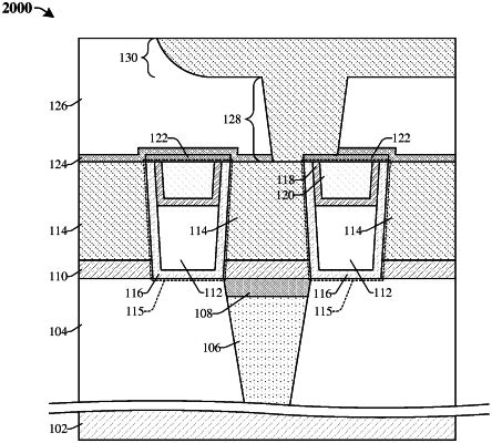
forming a dielectric structure laterally between the first conductive wire and the second conductive wire, wherein the dielectric structure comprises a first dielectric liner, a dielectric layer disposed between opposing sidewalls of the first dielectric liner, and a void between an upper surface of the first dielectric liner and a lower surface of the dielectric layer, wherein a top surface of the first dielectric liner is aligned with a top surface of the dielectric layer; and
forming a dielectric capping layer along an upper surface of the dielectric structure, wherein sidewalls of the dielectric capping layer are aligned with sidewalls of the dielectric structure.
|