| CPC H01L 23/49827 (2013.01) [H01L 21/486 (2013.01); H01L 21/78 (2013.01); H01L 23/49838 (2013.01); H01L 23/49894 (2013.01)] | 17 Claims |

|
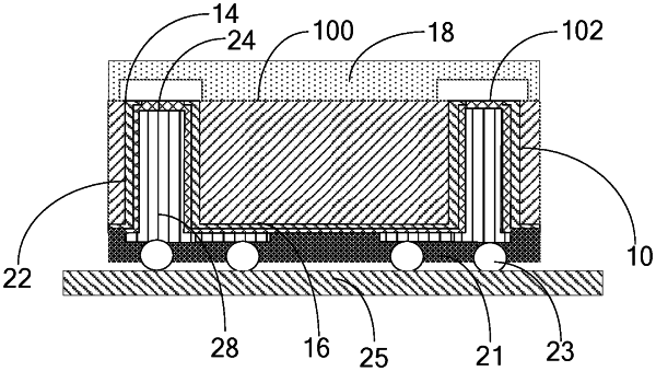
1. A semiconductor package device, comprising:
a chip substrate, having a front surface and a back surface, wherein the front surface includes a photosensitive region;
pads, disposed at the front surface of the chip substrate and around the photosensitive region, wherein the chip substrate contains through-holes at positions corresponding to the pads, and the through-holes one-to-one correspond to the pads;
a transparent protection layer, disposed over the front surface of the chip substrate and covering the photosensitive region and the pads;
a circuit board, electrically connected to each pad through a metal rewiring layer in a corresponding through-hole, wherein the metal rewiring layer is disposed over the back surface of the chip substrate and extended into the through-hole, and one end of the metal rewiring layer is electrically connected to the pad, and another end of the metal rewiring layer is electrically connected to the circuit board;
a first mask layer, disposed between the back surface of the chip substrate and the metal rewiring layer, wherein the first mask layer contains a first opening at a position corresponding to the pad; and
a first seed layer, disposed between the first mask layer and the metal rewiring layer, wherein the pad, the first seed layer, and the metal rewiring layer are electrically connected to each other.
|