| CPC H01L 23/49822 (2013.01) [H01L 23/49816 (2013.01); H01L 23/49838 (2013.01); H01L 23/49894 (2013.01); H01L 24/15 (2013.01)] | 20 Claims |
|
1. A semiconductor device comprising:
a wiring member including a plurality of wiring layers; and
a semiconductor chip electrically connecting with the wiring member,
wherein the plurality of wiring layers of the wiring member includes:
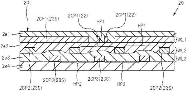
a first wiring layer having a plurality of first conductive patterns each covered with a first polyimide film,
a second wiring layer arranged next to the first wiring layer in a thickness direction of the wiring member, the second wiring layer having a second conductive pattern covered with a second polyimide film, and
a third wiring layer arranged next to the second wiring layer in the thickness direction of the wiring member, the third wiring layer having a third conductive pattern covered with a third polyimide film,
wherein the second wiring layer is arranged between the first wiring layer and the third wiring layer in the thickness direction of the wiring member,
wherein the plurality of first conductive patterns of the first wiring layer includes first and second differential signal wirings through which a differential signal is to be transmitted,
wherein the second conductive pattern of the second wiring layer is a first mesh pattern having a plurality of first opening portions, the plurality of first openings each penetrating through the second conductive pattern in the thickness direction of the wiring member,
wherein the third conductive pattern of the third wiring layer is a second mesh pattern having a plurality of second opening portions, the plurality of second opening portions each penetrating through the third conductive pattern in the thickness direction of the wiring member,
wherein the plurality of first opening portions of the second wiring layer includes two adjacent first opening portions, the two adjacent first opening portions being next to each other without having any first opening portions between the two adjacent first opening portions, and
wherein, in plan view, each of the two adjacent first opening portions of the second wiring layer overlaps the first differential signal wiring of the first wiring layer, the second differential signal wiring of the first wiring layer, and two or more second opening portions of the plurality of second opening portions of the third wiring layer.
|