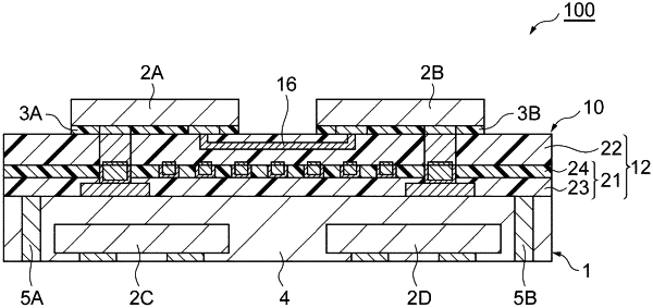
| CPC H01L 23/49822 (2013.01) [H01L 21/4857 (2013.01); H01L 23/12 (2013.01); H01L 23/145 (2013.01); H01L 23/32 (2013.01); H01L 23/49866 (2013.01); H01L 23/49894 (2013.01); H01L 23/5383 (2013.01); H01L 23/5384 (2013.01); H01L 23/5386 (2013.01); H01L 23/5389 (2013.01); H01L 25/0652 (2013.01); H01L 2225/06506 (2013.01); H01L 2225/06548 (2013.01); H01L 2225/06572 (2013.01); H05K 1/09 (2013.01)] | 20 Claims |

|
1. A substrate for a semiconductor package, comprising:
an organic insulating resin layer including a groove;
a first wire located in the groove;
a barrier conductive material covering the first wire; and
a second wire located above the first wire,
wherein the barrier conductive material includes:
a first barrier conductive film interposed between the first wire and the groove; and
a second barrier conductive film located on the first wire,
wherein the second wire is in contact with both of the first barrier conductive film and the second barrier conductive film; and
wherein an upper surface of the first wire is substantially aligned with an upper surface of the organic insulating resin layer.
|