| CPC H01L 23/49816 (2013.01) [H01L 24/11 (2013.01); H01L 24/13 (2013.01); H01L 24/14 (2013.01); H01L 24/16 (2013.01); H01L 24/81 (2013.01); H01L 2224/1319 (2013.01); H01L 2224/14179 (2013.01); H01L 2224/16227 (2013.01); H01L 2224/27849 (2013.01); H01L 2224/81815 (2013.01); H01L 2924/15311 (2013.01)] | 25 Claims |
|
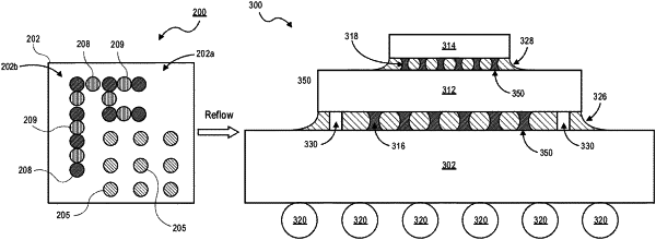
1. A semiconductor package, comprising:
a package substrate having a top surface, wherein the top surface includes a corner portion;
a plurality of solder balls on the top surface of the package substrate; and
a pattern on the corner portion of the package substrate, wherein the pattern has a width that is substantially equal to a width of the plurality of solder balls, wherein the pattern includes a continuous line, wherein the continuous line includes one or more solder materials, and wherein a solder composition of the continuous line varies along the continuous line.
|