| CPC H01L 23/49582 (2013.01) [H01L 21/4821 (2013.01); H01L 23/31 (2013.01); H01L 23/53242 (2013.01)] | 19 Claims |
|
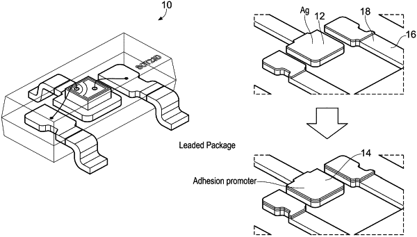
1. A semiconductor package comprising:
a lead frame having a lead frame surface;
an Ag plated surface positioned on the lead frame;
an adhesion promotion layer positioned on a top of the Ag plated surface; and
a mold body covering a top of the lead frame;
wherein the Ag plated surface covers a significant part of an interconnection area of the lead frame surface, and wherein the Ag plated surface does not substantially exceed an area of the mold body so that a portion of the lead frame surface extending beyond the area of the mold body is free from Ag plating.
|