| CPC H01L 23/49562 (2013.01) [H01L 23/3121 (2013.01); H01L 24/48 (2013.01); H01L 2224/48177 (2013.01)] | 20 Claims |
|
1. A semiconductor device, comprising:
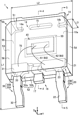
a substrate including a main surface;
a semiconductor element mounted on the main surface, the semiconductor element including a front surface that faces in a same direction as the main surface and a first electrode formed on the front surface and containing SiC;
a first pad arranged away from the substrate; and
wires spaced apart from each other and connecting the first electrode to the first pad, wherein
the wires include a first wire and a second wire configured to be a combination of furthermost ones of the wires,
the first wire and the second wire are connected to the first electrode and the first pad so that the first wire and the second wire are separated from each other by a greater distance at the first pad than at the first electrode as viewed in a first direction that is perpendicular to the main surface,
when a direction orthogonal to the first direction is a second direction, and a direction orthogonal to the first direction and the second direction is a third direction, the semiconductor element and the first pad are located at different positions in at least the second direction, the wires are spaced apart from each other in the third direction, and the first wire and the second wire are ones of the wires located at opposite ends in the third direction, and
the semiconductor device further comprises:
an insulation film formed on the first electrode; and
an opening formed in a portion of the insulation film to expose the first electrode, wherein
the opening is rectangular so that a short-side direction conforms to the second direction and a long-side direction conforms to the third direction as viewed in the first direction, and
a dimension of the first pad in the third direction is greater than a dimension of the opening in the third direction.
|