| CPC H01L 23/481 (2013.01) [H01L 23/5223 (2013.01); H01L 23/5226 (2013.01)] | 12 Claims |
|
1. A semiconductor structure, comprising:
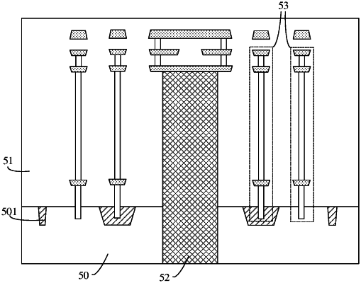
a substrate and a dielectric layer arranged on the substrate;
a conductive plug, a first part of the conductive plug being arranged in the substrate, and a second part of the conductive plug being arranged in the dielectric layer;
an isolation ring structure arranged in the substrate and in the dielectric layer, wherein the isolation ring structure surrounds the first part and the second part of the conductive plug; and
functional elements, wherein the functional elements are arranged outside a region enclosed by the isolation ring structure and are absent inside the region enclosed by the isolation ring structure,
wherein the isolation ring structure comprises at least one conductive pillar extending in a direction perpendicular to a surface of the substrate,
wherein the substrate comprises isolation structures, the at least one conductive pillar is arranged in the substrate, and a depth of the at least one conductive pillar in the substrate is equal to a depth of each of the isolation structures in the substrate.
|