| CPC H01L 23/3732 (2013.01) [H01L 23/562 (2013.01); H01L 24/32 (2013.01); H01L 24/83 (2013.01); H05K 3/3436 (2013.01); H05K 7/20254 (2013.01); H01L 25/0655 (2013.01); H01L 2223/58 (2013.01); H01L 2224/32 (2013.01); H01L 2224/32245 (2013.01); H01L 2924/15311 (2013.01); H05K 2201/10378 (2013.01); H05K 2203/041 (2013.01)] | 18 Claims |
|
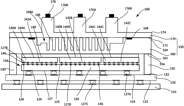
6. A method of manufacturing a chip assembly comprising:
joining an in-process unit to a printed circuit board, the in-process unit comprising:
a substrate having an active surface, a passive surface, and contacts exposed at the active surface;
an interposer electrically connected to the substrate;
a plurality of semiconductor chips overlying the substrate and electrically connected to the substrate through the interposer; and
a stiffener overlying the substrate and having an aperture extending therethrough, the plurality of semiconductor chips being positioned within the aperture;
reflowing a bonding material disposed between and electrically connecting the in-process unit with the printed circuit board, the bonding material having a first reflow temperature; and then
joining a heat distribution device to the plurality of semiconductor chips using a thermal interface material (“TIM”) having a second reflow temperature that is lower than the first reflow temperature,
wherein the heat distribution device further comprises a plurality of thermally conductive fins, wherein a first fin length of at least some of the plurality of thermally conductive fins is greater than a second fin length of remaining fins of the plurality of thermally conductive fins, wherein a first height of at least one of the plurality of semiconductor chips is less than a second height of others of the plurality of semiconductor chips, and
wherein the method further comprises positioning the at least some of the plurality of thermally conductive fins having a first fin length to overlie the at least one of the plurality of semiconductor chips having the first height.
|