| CPC H01L 23/3121 (2013.01) [H01L 21/56 (2013.01); H01L 23/3675 (2013.01); H01L 23/3736 (2013.01); H01L 23/481 (2013.01); H01L 23/528 (2013.01); H01L 23/5383 (2013.01); H01L 23/5386 (2013.01); H01L 23/66 (2013.01); H01L 24/16 (2013.01); H01L 24/81 (2013.01); H01L 25/072 (2013.01); H03F 1/0288 (2013.01); H03F 1/301 (2013.01); H03F 3/21 (2013.01); H01L 2223/6616 (2013.01); H01L 2223/6644 (2013.01); H01L 2224/16227 (2013.01); H01L 2224/8112 (2013.01); H01L 2224/81815 (2013.01); H03F 2200/451 (2013.01)] | 13 Claims |
|
1. A power amplifier module comprising:
a module substrate with a mounting surface, a first module pad exposed at the mounting surface, a second module pad exposed at the mounting surface, and a third module pad exposed at the mounting surface;
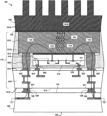
a first power transistor die with an input/output (I/O) surface, a ground surface opposite the I/O surface, an input pad exposed at the I/O surface, an output pad exposed at the I/O surface, and an integrated power transistor with a control terminal electrically coupled to the input pad, a first current-carrying terminal electrically coupled to the output pad, and a second current-carrying terminal electrically coupled to the ground surface, wherein the first power transistor die is coupled to the module substrate with the I/O surface facing the mounting surface, the input pad electrically coupled to the first module pad, and the output pad electrically coupled to the second module pad;
a first heat spreader with a first thermal contact surface, a second thermal contact surface, and sidewalls extending between the first and second thermal contact surfaces, wherein the first thermal contact surface includes an interior area and a peripheral area that extends parallel to the interior area between the interior area and a first sidewall of the sidewalls;
a patterned mask layer on the first thermal contact surface that includes an interior opening that exposes the interior area of the first thermal contact surface, and a peripheral opening that exposes the peripheral area of the first thermal contact surface, wherein the interior area is physically and electrically coupled through the interior opening to the ground surface of the first power transistor die; and
an electrical ground contact structure connected through the peripheral opening to the peripheral area of the first thermal contact surface, and also connected to the third module pad of the module substrate.
|