| CPC H01L 23/3107 (2013.01) [H01L 21/4853 (2013.01); H01L 21/561 (2013.01); H01L 21/566 (2013.01); H01L 21/568 (2013.01); H01L 21/6835 (2013.01); H01L 21/78 (2013.01); H01L 23/49811 (2013.01); H01L 24/11 (2013.01); H01L 24/94 (2013.01); H01L 24/97 (2013.01); H01L 25/10 (2013.01); H01L 21/4857 (2013.01); H01L 24/13 (2013.01); H01L 24/16 (2013.01); H01L 24/32 (2013.01); H01L 24/83 (2013.01); H01L 24/92 (2013.01); H01L 25/105 (2013.01); H01L 2221/68327 (2013.01); H01L 2221/68372 (2013.01); H01L 2224/12105 (2013.01); H01L 2224/13024 (2013.01); H01L 2224/13025 (2013.01); H01L 2224/131 (2013.01); H01L 2224/16225 (2013.01); H01L 2224/2919 (2013.01); H01L 2224/32225 (2013.01); H01L 2224/73253 (2013.01); H01L 2224/83005 (2013.01); H01L 2224/92242 (2013.01); H01L 2224/97 (2013.01); H01L 2225/1035 (2013.01); H01L 2225/1041 (2013.01); H01L 2225/1058 (2013.01); H01L 2924/15311 (2013.01); H01L 2924/15321 (2013.01); H01L 2924/181 (2013.01); H01L 2924/19107 (2013.01)] | 22 Claims |
|
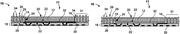
1. A microelectronic assembly having a first side and a second side opposite from the first side, the microelectronic assembly comprising:
a first microelectronic element having a first face, a second face opposite the first face, a plurality of sidewalls each extending between the first and second faces, and a plurality of element contacts at the first face;
an encapsulation adjacent the sidewalls of the first microelectronic element and having a thickness in a direction between the first and second sides of the microelectronic assembly;
electrically conductive connector elements each positioned beyond an end of the first microelectronic element and each having a first end, a second end remote from the first end, and a surface extending between the first and second ends, wherein one of the first end or the second end of each connector element is adjacent the first side of the microelectronic assembly, the surface of each connector element being contacted by the encapsulation between the first and second ends;
a redistribution structure comprising electrically conductive traces, the redistribution structure built up layer-by-layer over the encapsulation and connector elements and overlying both the encapsulation and the first microelectronic element, the other of the first end or the second end of each connector element being electrically coupled with the conductive traces of the redistribution structure; and
a second microelectronic element between the redistribution structure and the second side of the microelectronic assembly, the second microelectronic element coupled to the redistribution structure through conductive masses.
|