| CPC H01L 22/20 (2013.01) [H01L 27/124 (2013.01); H01L 27/1244 (2013.01); H01L 27/1288 (2013.01); G02F 1/136259 (2013.01); G02F 1/1368 (2013.01)] | 20 Claims |
|
7. A manufacturing method of an array substrate, comprising following steps:
providing a substrate;
forming a first metal layer on the substrate;
etching the first metal layer to form a hollow area;
forming a gate insulation layer on the first metal layer;
forming a semiconductor layer on the gate insulation layer, wherein the semiconductor layer comprises a first area and a second area, and a vertical projection of an area between the first area and the second area on the substrate completely covers a vertical projection of the hollow area on the substrate; and
forming a second metal layer on the semiconductor layer;
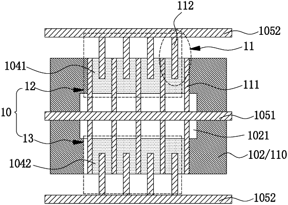
wherein the first metal layer, the gate insulation layer, the semiconductor layer, and the second metal layer together become at least one switch unit, each of the switch unit comprises a plurality of thin film transistors (TFTs) in parallel, and each of the switch unit comprises at least two columns of a first TFT set and at least two columns of a second TFT set.
|