| CPC H01L 21/823814 (2013.01) [H01L 21/28518 (2013.01); H01L 21/823821 (2013.01); H01L 21/823871 (2013.01); H01L 21/823878 (2013.01); H01L 27/0924 (2013.01); H01L 29/0653 (2013.01); H01L 29/0847 (2013.01); H01L 29/41791 (2013.01); H01L 29/45 (2013.01); H01L 29/66545 (2013.01); H01L 29/66636 (2013.01); H01L 29/66795 (2013.01); H01L 29/7851 (2013.01)] | 18 Claims |

|
1. A method comprising:
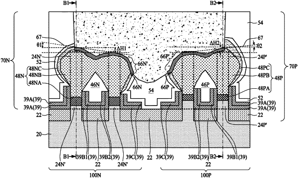
forming isolation regions extending into a semiconductor substrate;
forming a first plurality of protruding fins and a second protruding fin over the isolation regions, wherein the first plurality of protruding fins comprise an outer fin farthest from the second protruding fin, and an inner fin closest to the second protruding fin;
etching the first plurality of protruding fins to form first recesses;
growing first epitaxy regions from the first recesses, wherein the first epitaxy regions are merged to form a merged epitaxy region;
etching the second protruding fin to form a second recess; and
growing a second epitaxy region from the second recess, wherein a first top surface of a first outmost part of the merged epitaxy region grown from a first outmost one of the first recesses is lower than a second outmost part of the merged epitaxy region grown from a second outmost one of the first recesses, and wherein the first outmost part faces toward the second epitaxy region, and the second outmost part faces away from the second epitaxy region.
|